


Electron. Mater. 2024, 5(2), 56-70; https://doi.org/10.3390/electronicmat5020005 - 13 May 2024
Abstract
►
Show Figures
All-inorganic perovskite semiconductors have received significant interest for their potential stability over heat and humidity. However, the typical CsPbI3 displays phase instability despite its desirable bandgap of ~1.73 eV. Herein, we studied the mixed halide perovskite CsPbI2Br by varying the
[...] Read more.
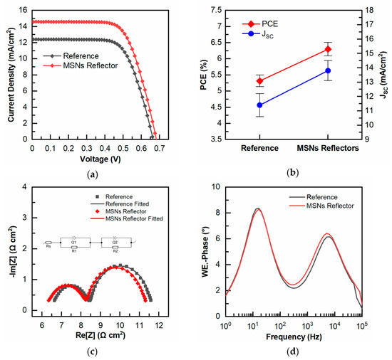
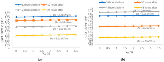
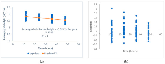
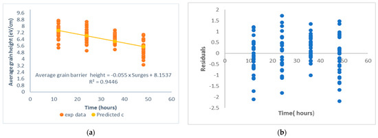
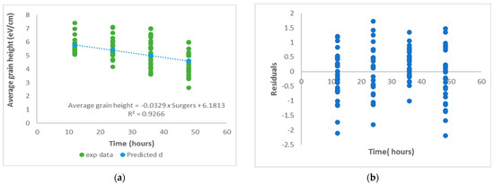
All-inorganic perovskite semiconductors have received significant interest for their potential stability over heat and humidity. However, the typical CsPbI3 displays phase instability despite its desirable bandgap of ~1.73 eV. Herein, we studied the mixed halide perovskite CsPbI2Br by varying the silver doping concentration. For this purpose, we examined its bandgap tunability as a function of the silver doping by using density functional theory. Then, we studied the effect of silver on the structural and optical properties of CsPbI2Br. Resultantly, we found that ‘silver doping’ allowed for partial bandgap tunability from 1.91 eV to 2.05 eV, increasing the photoluminescence (PL) lifetime from 0.990 ns to 1.187 ns, and, finally, contributing to the structural stability when examining the aging effect via X-ray diffraction. Then, through the analysis of the intermolecular interactions based on the solubility parameter, we explain the solvent engineering process in relation to the solvent trapping phenomena in CsPbI2Br thin films. However, silver doping may induce a defect morphology (e.g., a pinhole) during the formation of the thin films.
Full article

Figure 1


